32-bit RISC CPU & FPGA Pong
Verilog / Vivado / FPGA / Computer Architecture
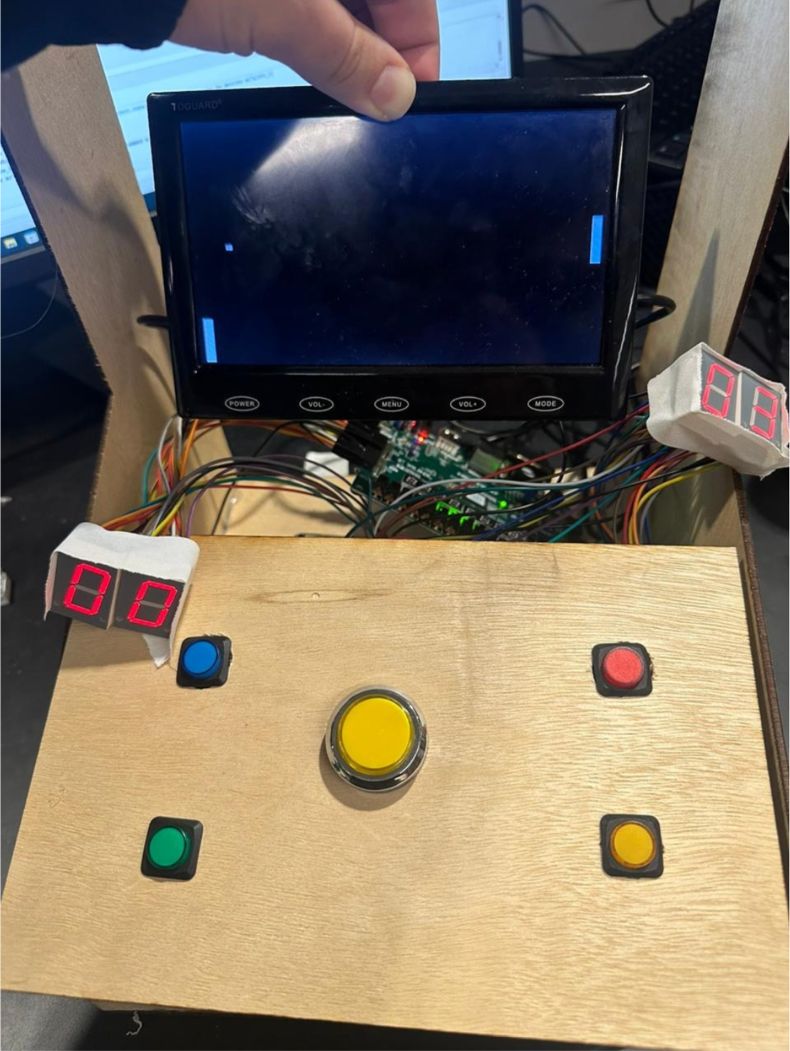
A 32-bit RISC processor with a MIPS-based ISA, written from scratch in Verilog and synthesized onto a Xilinx FPGA at 100MHz. To prove the whole stack works, it runs a Pong clone written in assembly, rendered over VGA with live keyboard input.
Implementation Details
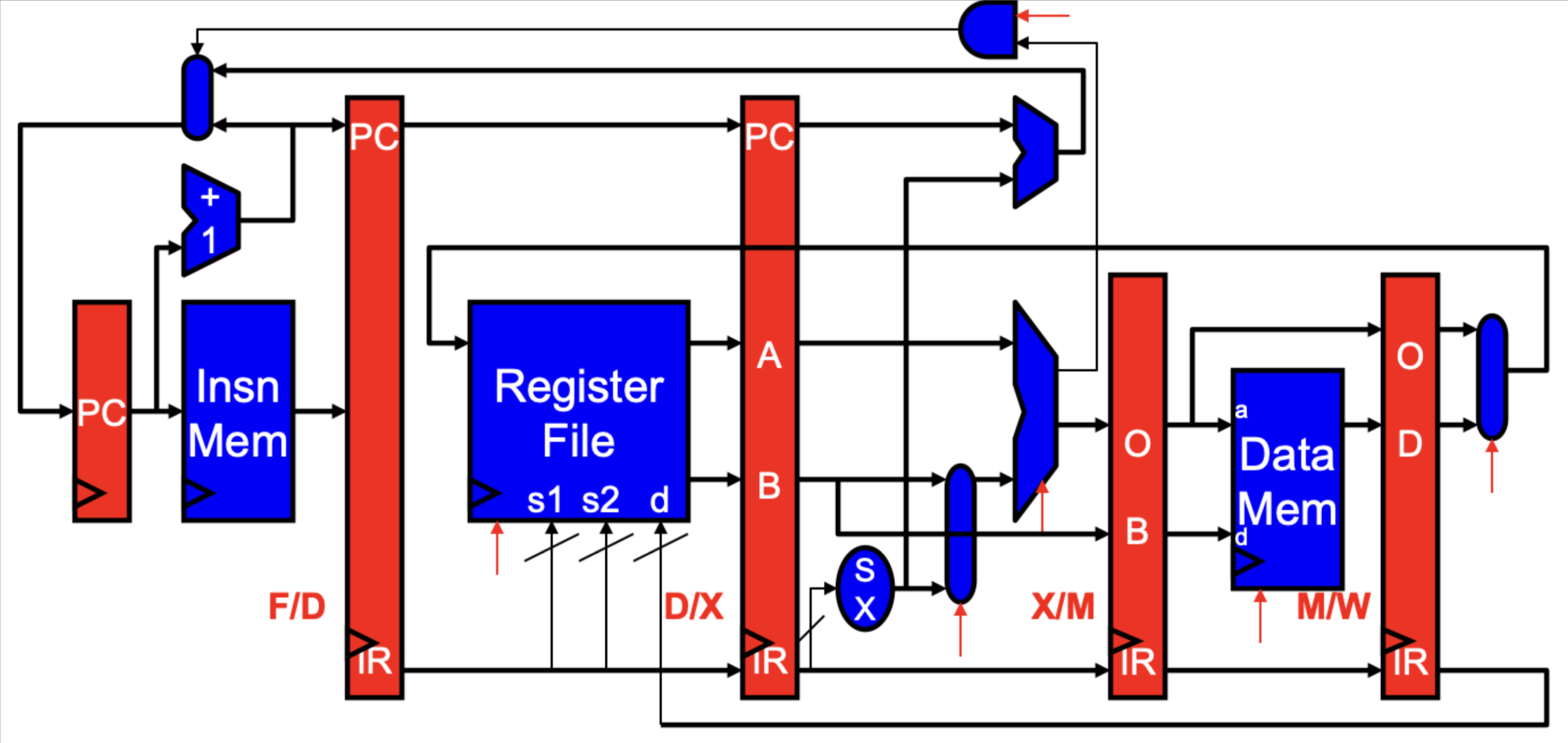
The core is a five-stage pipelined RISC processor comprising Fetch, Decode, Execute, Memory, and Writeback stages. We implemented full hazard detection logic to maintain throughput. A forwarding unit compares the destination registers in the Memory and Writeback stages against the source registers in the Decode stage. If a match is found, the data is bypassed directly to the ALU inputs to resolve Read-After-Write hazards. For Load-Use hazards where bypassing is impossible, a stall unit inserts NOP bubbles into the pipeline.
The system interfaces with a custom VGA controller driven by a 25MHz pixel clock divided from the 100MHz system clock. We utilized memory-mapped I/O to expose the video memory and PS/2 keyboard state to the processor's address space. The Pong game logic is written in MIPS assembly. It polls the keyboard address for paddle input and updates the ball coordinates by writing to specific VGA memory addresses. A hardware divider facilitates the ball angle calculations, and the software handles game state, letting players select single-player (against an AI paddle) or multiplayer mode from an initial menu screen. The design synthesizes onto a Xilinx FPGA, utilizing block RAM for instruction and data memory.